BRN Discussion Ongoing

Slymeat

Move on, nothing to see.
didn't want to confuse anyone. but since we have a partnership with AirForce about the development of a radar system. I thought to share an article where you can see where this can go. Which by the way is new and is currently being discussed a lot on TV.
Thanks for clearing that up @Dallas. I must admit that I did originally fail to see the link.

I do hope Akida is involved in its AI.

Now that WOULD be sweet.
 
  • Like
Reactions: 4 users

Dhm

Regular
I did hear of the ResApp approach being debunked somewhat due to the fact that many covid sufferers do not have a cough. Many sufferers are completely asymptomatic. DISC: I hold shares in ResApp.

The Nanose /diaNose approach of detecting Volatile Organic Compounds seems, IMHO, to be where the future lies.
Debunked by people who don't understand the tech and sensitivity of the lungs when they get the virus. A forced cough still has the alveoli irritation that Covid causes and therefore the algorithms detect. Anyway this isn't the place to comment on other companies.

As you say, the Nanose Brainchip technology will be where much of the future lies.
 
  • Like
Reactions: 4 users

Slymeat

Move on, nothing to see.
Debunked by people who don't understand the tech and sensitivity of the lungs when they get the virus. A forced cough still has the alveoli irritation that Covid causes and therefore the algorithms detect. Anyway this isn't the place to comment on other companies.

As you say, the Nanose Brainchip technology will be where much of the future lies.
The post I read was written by a medical doctor and that was sufficient for me.

Being a long suffering ResApp shareholder, I did have my rose-tinted glasses firmly on at the time too.

And although I was merely replying to your original post on a technology that does not involve Akida, I do believe it is OK to mention other technologies/companies that may be in competition to technologies that incorporate Akida. That creates a healthy discussion.
 
  • Like
Reactions: 6 users

LuWil

Regular

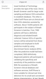
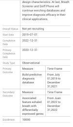
Cancer Diagnoses From Exhaled Breath With Na-nose​


Completion date: 31/12/2022
 

Attachments

  • D7399A04-15B1-4AD3-B0F7-15E939832180.jpeg
    D7399A04-15B1-4AD3-B0F7-15E939832180.jpeg
    251.2 KB · Views: 106
  • 7E82A483-3BCB-4E68-8AD4-2F16967FA773.jpeg
    7E82A483-3BCB-4E68-8AD4-2F16967FA773.jpeg
    265.5 KB · Views: 99
  • 60B38A41-282E-4828-8281-210D2D83DFBE.jpeg
    60B38A41-282E-4828-8281-210D2D83DFBE.jpeg
    190.2 KB · Views: 99
  • Like
Reactions: 2 users

Diogenese

Top 20
I thought this was interesting. This fellow worked at Hewlett-Packard Back then for around 12 years and as you will see has a belief in neuromorphic computing. If you only give him a credibility rating of 50% to account for the issues around social media what Brainchip has achieved to date is well beyond astounding.
My opinion only DYOR
FF

AKIDA BALLISTA
View attachment 3265
https://www.quora.com/How-far-along-is-neuromorphic-computing
How far along is neuromorphic computing?
It’s no less than 20 years out. I regularly attend IEEE meetings related to the core technologies and its manufacture. I also work with organizations likely to be the first to adopt.
We haven't figured out the basic details of the devices required to make neuromorphic neural nets yet. We have ideas of what likely will work but these devices are still Big-Research, Little-Product Development (R & d), rather than Little-R, Big-D.
The devices that have been built are not reliable enough to be used commercially yet. There are issues with manufacturability and quality. There is infrastructure uncertainty and market uncertainty still - everyone promises they’ll buy product but until they actually do, they could be blowing smoke up your posterior.
We don’t yet have test equipment capable of testing many of the fundamental performance metrics of these devices. Developing the latter will still take 5–10 years if we could get a firm spec for what is required and the numbers we have so far tell us WE need several years of R&D ourselves as upstream suppliers to these researchers just to figure out how to make such equipment and make it useable.
We have at least started toward this technology but there are many, many critical path issues unsolved and undefined still. It’s not an economically viable reality yet. It’s still pure research. This is actually 100% normal for early stage pre-technologies. In general, you have a 20 year timer that only starts once you’ve proven all the key underlying technologies.
The short answer: getting a PhD in the area (which takes 5–10 years) is still a good idea if you want to do that. Many PhD-level questions still need to answered first/yet!

Well Jeff was clearly talking about analog NNs (ReRAM/MemRistors).

"There are issues with manufacturability and quality."

One of PvdM's great insights eliminated these problems at one stroke - a digital NN that uses standard CMOS manufacturing and binary digital signals. While analog neurons are a close theoretical analogy to real neurons, manufacturing variability is still one of the issues that analog NN makers still have to address because any variations in component dimensions alters the amplitude of the analog signals because the strength of the various current signals are added to determine when the firing threshold is reached. The current strength is determined by the tolerance of the resistors/capacitors. So, by way of an illustrative example only, if there were say a 10% variation in signal strengths, adding just 5 analog signals could produce a chance of up to 50% error in the sum of the signal strengths.

On the other hand, binary digital circuits have a high tolerance for manufacturing variations as each switching element produces either a 1 or a zero output. The supply voltage of a CMOS transistor would be much higher than +/- 10% of the trigger threshold voltage.

As for the test equipment, there are the various image databases against which the performance of NNs can be gauged.

I'll leave it to others, like Socionext, Mercedes, Renesas, MegaChips, Valeo, NASA ... to assess the market uncertainty and economic viability.

I blame ill-conceived KIPs for the siloization of work. In the old days, you could always peek over your neighbour's fence to see what was happening elsewhere. I'm pretty sure Crick & Watson did not have KIPs when they were tossing ideas around in a Cambridge pub.
 
  • Like
  • Fire
  • Love
Reactions: 17 users

Yoda

Regular
Most certainly there is money in automotive for Brainchip but remember the acting CEO Peter van der Made, the then VP of Sales and Marketing Rob Telson put forward last year that they were going to saturate the Edge market. Not we are going to saturate an Edge market. They also used the word ubiquitous to describe what they had planned for AKIDA and did not qualify it as just being the automotive market where this was going to happen. The new CEO Sean Hehir has not stated otherwise than his one comment about focus.

Then we have both Renesas and MegaChips who cover more than just automotive and MegaChips actually list mobile phones as a potential use case for AKIDA technology.

Then there is the Nanose SniffPhone idea which clearly needs a mobile phone to fulfil the description.

There are so many other Smart Health applications which can be processed through mobile phones but if they cause the phone to need a recharge every 30 minutes are likely not going to be picked up but a 3 to 5 day phone life they become the marketing edge for a phone company.

I was reading an article yesterday probably posted here by someone but it was basically saying that do not expect your new phone to be much more revolutionary than the last one because battery life was greatly restricting added innovations.

I am not saying Brainchip is in bed with a mobile phone company but I am saying it cannot be discounted on the basis of known facts.

Also on the Mercedes EQXX front remember the concept also includes turning it into a technology hub linked to your Smartphone, your Smartoffice, your Smarthome it could be argued that just this one known fact makes it more likely than not that phones using AKIDA technology are already on the table.

My opinion only DYOR
FF

AKIDA BALLISTA
Throwing the question out there, but how much (if any) revenue from these activities do you think we will see in the next quarterly? Or are we still too early for any significant revenue ?
 
  • Like
Reactions: 3 users

Foxdog

Regular
Who is looking forward to Ford breaking cover and saying they have “Akida Inside” 😁.

Surely they want to be looking as cool and EV competitive as Mercedes soon!
I'm looking forward to Ford vs Mercedes in a hot lap. Then imagine an entire grid full of autonomous race cars each with AKIDA - perhaps not so fanciful....
 
  • Like
  • Wow
  • Haha
Reactions: 9 users

MrNick

Regular
I'm looking forward to Ford vs Mercedes in a hot lap. Then imagine an entire grid full of autonomous race cars each with AKIDA - perhaps not so fanciful....
That's sounds about as enjoyable and gonad-fizzy as watching Formula E.
 
  • Like
  • Haha
Reactions: 6 users

Bravo

If ARM was an arm, BRN would be its biceps💪!
Voago Linkedin 2 days ago.


Screen Shot 2022-03-28 at 12.03.07 pm.png


This made me think about FF's post about Nokia being chosen by NASA to deploy the first LTE/4G communications system on the Moon. I'm certainly no expert but I'm assuming that the hardware that Nokia intend to use will need to be space-hardened. Vorago, Nockia and BrainChip - a match made in heaven (or on the moon) one would think. :p


(Extract 1 - BrainChip and VORAGO Technologies Agree to Collaborate through the Akida™ Early Access Program)

Louis DiNardo, BrainChip CEO commented, “We are both excited and proud to participate in this Phase I program with VORAGO Technologies and support NASA’s desire to leverage neuromorphic computing in spaceflight applications. The combination of benefits from the Akida neuromorphic processor and a radiation-hardened process brings significant new capabilities to spaceflight and aerospace applications”.


Bernd Lienhard, VORAGO CEO added, “We are thrilled and honored to partner with BrainChip to harness the radiation hardening capabilities of our patented HARDSIL® technology for the Phase I program with NASA. Our ongoing mission of creating components with increased availability and unmatched solutions in aerospace and defense applications paired with the Akida neuromorphic processor will create unprecedented standards moving forward in the industry.”


(Extract 2 - Thierry Klein, head of Enterprise and Industrial Automation Research Lab at Nokia Bell Labs, is addressing the gap between communication technology on the Moon and technology astronauts have access to on Earth. )


VIA SATELLITE: What are the challenges to building a network on the Moon? It sounds like science fiction. How difficult will this be?​


Klein: The main challenge is the environment. We know how to build the core 4G and LTE systems and how to transmit data wirelessly. The first challenge is all of the space hardening, whether it is for the launch of the rocket, the landing on the Moon, or the extreme mechanical stress that the equipment will be exposed to in terms of shock, vibration, and acceleration.


We also need to harden the equipment for the unique space environment, like the extreme hot and cold temperatures, the vacuum, radiation, and the impact of radiation on the equipment. That is a really difficult problem.


I would say the third challenge comes from the operational environment. We need to be very meticulous about size, weight, and power consumption. We need to worry about integrating our network equipment with the lunar lander and integration with the lunar rover. We need to have a fully operational system that is reliable and robust because we can’t send a technician to the Moon to make configuration changes or reboot the system. The system has to be completely autonomous and we need to be able to remotely monitor, manage, and configure it from mission control on Earth.


  • Like
  • Fire
  • Love
Reactions: 30 users
Throwing the question out there, but how much (if any) revenue from these activities do you think we will see in the next quarterly? Or are we still too early for any significant revenue ?
I recently had a private conversation with another poster on this question and extracting the relevant part the following is my view which I referred to Tony Dawe at the time to be sure I was not completely off the mark and he responded that he saw no reason to change my response:

"When Sean Hehir was interviewed earlier this year he answered Yes to a question about would revenue start to ramp up this year.

I personally have never expected explosive income growth this year but there are stages in a company like Brainchip's development.

1. The first is the development phase and during this phase there is no income and going concern status is determined by capital raises.

2. The second stage is becoming a commercial entity and then the income is a mix of capital raises and some income.

3. The third stage is becoming a going commercial concern where its continued operation is being funded from income and capital raises if required are only for special projects or acquisitions and not to meet day to day operating expenses.

4. The fourth stage is when the income increases beyond simply funding ongoing operations and questions of what shall it do with profits arise.

The messages I have been hearing from Brainchip have communicated to me that we are in the second stage and the third stage will start second half of this year.

I personally had no expectation of explosive revenue occurring this year. What I do expect from Peter van der Made's explosive sales statement is that we will see an increasing number of current EAP's breaking cover and more and more logo's of companies appearing in the Early Adopters and Licensee columns and license fees will be seen in the balance sheet. We will also likely see other companies making announcements similar to Mercedes."


My opinion only DYOR
FF

AKIDA BALLISTA
 
  • Like
  • Fire
  • Love
Reactions: 65 users

Slade

Top 20
Too long down rabbit holes for me. What I learned was that Driver Monitoring Systems are likely to be mandated just like seat belts. With the need for low power and privacy I would say Akida is in pole position.
From our website:
The Akida AKD1000 Edge AI processor can also monitor the passenger compartment, checking driver alertness with the aim to reduce human error. Privacy is assured without the need to upload images to the internet.
 
  • Like
  • Fire
  • Love
Reactions: 22 users

Diogenese

Top 20
An interesting report and pages 17 & 18 relating to HRL and on phone cybersecurity are particularly interesting. @Diogenese might like to do a little patent searching to see how they are using STDP???


My opinion only DYOR
FF

AKIDA BALLISTA

"Unlike existing approaches, iSentinel utilizes three stages for anomaly detection with low false alarms: (1) the neuromorphic chip for continuous online monitoring and classification, (2) our EWS algorithms run on the mobile device CPU for closer inspection of alerts, and (3) the offline backend server for group behavior analysis"

HRL Labs have a couple of relevant patents/applications.

US10986113 is directly related to the article.

They do not describe their neurons or NPU, but their custom NN contains 576 neurons, so this does not exclude the use of Akida IP.

As to STDP, they use it and "neuron" in the manner of res ipsa loquiter, something which would displease Ella.

US10986113B2 System for continuous validation and threat protection of mobile applications

equivalent to WO2019147330A1 SYSTEM FOR CONTINUOUS VALIDATION AND PROTECTION OF MOBILE APPLICATIONS

1648431285631.png


1648431157376.png


Described is a low power system for mobile devices that provides continuous, behavior-based security validation of mobile device applications using neuromorphic hardware. A mobile device comprises a neuromorphic hardware component that runs on the mobile device for continuously monitoring time series related to individual mobile device application behaviors, detecting and classifying pattern anomalies associated with a known malware threat in the time series related to individual mobile device application behaviors, and generating an alert related to the known malware threat. The mobile device identifies pattern anomalies in dependency relationships of mobile device inter-application and intra-applications communications, detects pattern anomalies associated with new malware threats, and isolates a mobile device application having a risk of malware above a predetermined threshold relative to a risk management policy.

[0094] In one embodiment, a neuromorphic chip 306 is used in the first stage 310 of the system. There are several unique features of the hardware design. First, the hardware 306 computes with spikes 320 (fixed voltage pulses of very narrow width (i.e., on the order of 1-2 ms) rather than analog or digital encoding. This mode of encoding is data agnostic and is orders of magnitude more energy efficient compared to a digital system since it only consumes energy during the generation of spikes 320 . Spiking hardware 306 represents signals based on the inter-spike intervals and, thus, is more area efficient since it requires a single wire to encode and transmit information unlike digital systems. Finally, it is more scalable than pure analog systems as spike based systems only require to transmit the timing but not both timing and amplitude parts of the signal in large scale systems

[0095] Various models and algorithms have been developed that can compute with spikes 320 and, in particular, have shown that these models can perform multimodal pattern clustering and recognition as well as associative memories with high storage capacity. For instance, the on-chip learning capabilities can enable the neuromorphic chip 306 to be deployed in one of three modes of operation: unsupervised learning mode (see Literature Reference No. 33) where there is no human in the loop or ground truth, supervised learning mode (see Literature Reference No. 34) where the user can train the chip 306 to learn (for example the classes of objects) and then deployed after the learning is completed or in a reinforcement learning mode (see Literature Reference Nos. 35 and 40), where the chip 306 receives periodic quality of performance feedback (for example, good, bad, etc.) that enables the neuromorphic chip 306 to adapt and learn on-chip. This on-chip learning capability also offers minimal programming, interfacing and software cost while enabling rapid prototyping possibilities. The inputs to the chip 306 will be in the form of spike trains (element 320 ) encoded offline and then fed to the chip 306 , and the neural network on the chip 306 will process the incoming spikes 320 .

[0096] In this mode of operation, the chip 306 functions as a plastic reservoir where the synapses between neurons in the reservoir adapt the gain on the synapses based on spike timing dependent plasticity (STDP). This process is akin to a nonlinear and high-dimensional projection of sensory data into a spatio-temporal space where the data can be readily separated using linear decision boundaries. More specifically, during training, to realize the linear decision boundaries, the spiking activity of a subset of the neurons in the chip 306 is decoded via the output pads and performs a linear regression based learning operation, wherein the firing rates of the neurons sampled at the output pads are linearly combined to cause an output label neuron to fire.

[0098] ... Each synapse includes a weight adaptation circuit based on STDP. To operate, the chip custom boards are specified. These boards are used to interface the chip 306 with a computer. The boards can be used for initial evaluation of different processing neural networks in the chip 306

[0102] The 576-neuron neuromorphic hardware 306 described above has been utilized to perform learned classification of input signals. FIG. 7 depicts a random neural net as configured on a
576-neuron neuromorphic chip.

########################################################

US9336239 is a much earlier HRL patent which also relates to cyber security, and may have been the original basis for the above, albeit it uses "conventional computer" neural network software, possibly something like BrainChip Studio.

US9336239B1 System and method for deep packet inspection and intrusion detection

The present invention relates to a system for deep packet inspection and intrusion detection. The system uses a pattern matching module receiving as an input a data stream in a neural network. Neurons are activated such that when active, the neuron fires to all connecting output neurons to form a neuron spike, each neuron spike from the assigned neuron to a connecting output neuron having a delay. A delay is associated with each input character in the pattern, such that a position of each input character relative to an end of the pattern is stored in an alphabet-pattern-delay matrix (APDFM). An activation matrix (AM) is used to match each input character with a stored pattern to generate a similarity match and determine if the string of characters is the stored pattern.


[0001] This is a Continuation-in-Part application of U.S. Non-Provisional Application No. 13/358,095, filed on Jan. 25, 2012, and entitled, “Neural Network Device with Engineered Delays for Pattern Storage and Matching,” which is a non-provisional application of U.S. Provisional Application No. 61/501,636, filed on Jun. 27, 2011 and entitled, “Neural Network Device with Engineered Delays for Pattern Storage and Matching.”

[0002] This is ALSO non-provisional patent application of U.S. Provisional Application No. 61/589,666. filed on Jan. 23, 2012, entitled, “System and Method for Deep Packet Inspection and Intrusion Detection.”

[0015] ... For example, the system receives as an input a data stream in a neural network. The data stream has a sequence of characters in a pattern and is received in the neural network such that at each time t, only a single input character is received. Each single input character assigned to a neuron in the neural network. The neuron assigned to the single character is activated such that when active, the neuron fires to all connecting output neurons to form a neuron spike, with each neuron spike from the assigned neuron to a connecting output neuron having a delay. A delay associated with each input character in the pattern is determined, such that a position of each input character relative to an end of the pattern is stored in an alphabet-pattern-delay matrix (APDFM). Finally, using an activation matrix (AM), each input character is matched with a stored pattern to generate a similarity match, such that if the similarity match exceeds a predetermined threshold, the sequence of characters in the input data stream is identified as the stored pattern
.


[0061] ... the present invention is directed to an intrusion detection system that is operable for performing Deep Packet Inspection (DPI) at wire speeds in software running on conventional processors. The system uses an underlying detection engine (MagicNet) that is based on the relatively new theory of polychronous spiking neural models. The system uses a new and different paradigm than other recent spiking models and liquid state machines in that the network conduction delays are set to optimize detection of specific known patterns of interest (exact pattern matching). By setting the network conduction delays, the system is adapted to provide a more efficient detection than previous methods. In special purpose parallel hardware or a neuromorphic implementation, the system and method is operable for detecting attack signatures at wire speeds greater than 1 Tbps, and with much lower size, weight, and power than conventional methods.

1648432941117.png
 
  • Like
  • Fire
  • Wow
Reactions: 14 users

Bravo

If ARM was an arm, BRN would be its biceps💪!
Voago Linkedin 2 days ago.


View attachment 3297


This made me think about FF's post about Nokia being chosen by NASA to deploy the first LTE/4G communications system on the Moon. I'm certainly no expert but I'm assuming that the hardware that Nokia intend to use will need to be space-hardened. Vorago, Nockia and BrainChip - a match made in heaven (or on the moon) one would think. :p


(Extract 1 - BrainChip and VORAGO Technologies Agree to Collaborate through the Akida™ Early Access Program)

Louis DiNardo, BrainChip CEO commented, “We are both excited and proud to participate in this Phase I program with VORAGO Technologies and support NASA’s desire to leverage neuromorphic computing in spaceflight applications. The combination of benefits from the Akida neuromorphic processor and a radiation-hardened process brings significant new capabilities to spaceflight and aerospace applications”.


Bernd Lienhard, VORAGO CEO added, “We are thrilled and honored to partner with BrainChip to harness the radiation hardening capabilities of our patented HARDSIL® technology for the Phase I program with NASA. Our ongoing mission of creating components with increased availability and unmatched solutions in aerospace and defense applications paired with the Akida neuromorphic processor will create unprecedented standards moving forward in the industry.”


(Extract 2 - Thierry Klein, head of Enterprise and Industrial Automation Research Lab at Nokia Bell Labs, is addressing the gap between communication technology on the Moon and technology astronauts have access to on Earth. )


VIA SATELLITE: What are the challenges to building a network on the Moon? It sounds like science fiction. How difficult will this be?​


Klein: The main challenge is the environment. We know how to build the core 4G and LTE systems and how to transmit data wirelessly. The first challenge is all of the space hardening, whether it is for the launch of the rocket, the landing on the Moon, or the extreme mechanical stress that the equipment will be exposed to in terms of shock, vibration, and acceleration.


We also need to harden the equipment for the unique space environment, like the extreme hot and cold temperatures, the vacuum, radiation, and the impact of radiation on the equipment. That is a really difficult problem.


I would say the third challenge comes from the operational environment. We need to be very meticulous about size, weight, and power consumption. We need to worry about integrating our network equipment with the lunar lander and integration with the lunar rover. We need to have a fully operational system that is reliable and robust because we can’t send a technician to the Moon to make configuration changes or reboot the system. The system has to be completely autonomous and we need to be able to remotely monitor, manage, and configure it from mission control on Earth.


Also, Boeing is building the core stages for Artemis II and III, which is a bit interesting too.

Oh, and apparently the Space Launch System has 500 sensors. I wonder how many of them are AKIDA?


Screen Shot 2022-03-28 at 1.06.31 pm.png
Screen Shot 2022-03-28 at 1.20.22 pm.png


  • Like
  • Fire
Reactions: 12 users
Seems like he's talking about devices more so than a chip... was it Sean that said the chip is going into things the world hasn't even seen yet?
He's an electrical engineer not a neuromorphic scientist I noticed..
Hi Alfie
I was unsure from all your previous posts to what extent you understand the topic of neuromorphic computing as you write with such a definite approach to subjects but from this reply it seems you might be helped by the following two items.

The first is taken from Wiki:

“Neuromorphic engineering is an interdisciplinary subject that takes inspiration from biology, physics, mathematics, computer science, and electronic engineering[5] to design artificial neural systems, such as vision systems, head-eye systems, auditory processors, and autonomous robots, whose physical architecture and design principles are based on those of biological nervous systems.[10] It was developed by Carver Mead[11] in the late 1980s.”

The second is a link to an article about neuromorphic engineering:


The reality is there is no such thing yet as a neuromorphic scientist. The closest thing we have in the world of academia is an Engineer who has made a study of neuromorphic computing. As these articles however make clear mostly in universities the study of neuromorphic computing has been in terms of analogue not digital computing though in the last couple of years I have observed that there are now a few universities that offer engineering degrees that have added a subject that covers to some extent digital spiking neural networks.

The great luck that we have here is that we have a retired highly credentialed engineer with a background in patent law who goes by the name of @Diogenese. Diogenese makes the point that sometimes the discussion surrounding neuromorphic computing is above his pay grade and this is only to be expected as he went to university quite a few years ago now but having said this if it is above his pay grade then 99% of us here have not got a chance of understanding it any better.

The point of my post hence the 50% discount I referred to was that as recently as 2020 a mainstream engineer with Hewlett Packard who obviously from his statements had been taking a solid interest in neuromorphic computing had absolutely no inkling that Brainchip and the AKIDA technology solution existed in the real world as Intellectual Property and that a chip AKD1000 was due for release in October, 2020 the year he wrote his little reply.

I did assume Quora provide accurate numbers so it can be seen from his profile that his responses on that forum which is inhabited by a lot of qualified individuals including engineers in the field of computing have read his thoughts 6.4 million times.

He of course may not know anything at all about neuromorphic computing and is just shooting from the hip but if so it is not because he is not a neuromorphic scientist and goes to illustrate the overall point I was making.

My opinion only DYOR
FF

AKIDA BALLISTA
 
Last edited:
  • Like
  • Fire
  • Love
Reactions: 17 users
"Unlike existing approaches, iSentinel utilizes three stages for anomaly detection with low false alarms: (1) the neuromorphic chip for continuous online monitoring and classification, (2) our EWS algorithms run on the mobile device CPU for closer inspection of alerts, and (3) the offline backend server for group behavior analysis"

HRL Labs have a couple of relevant patents/applications.

US10986113 is directly related to the article.

They do not describe their neurons or NPU, but their custom NN contains 576 neurons, so this does not exclude the use of Akida IP.

As to STDP, they use it and "neuron" in the manner of res ipsa loquiter, something which would displease Ella.

US10986113B2 System for continuous validation and threat protection of mobile applications

equivalent to WO2019147330A1 SYSTEM FOR CONTINUOUS VALIDATION AND PROTECTION OF MOBILE APPLICATIONS

View attachment 3299


View attachment 3298

Described is a low power system for mobile devices that provides continuous, behavior-based security validation of mobile device applications using neuromorphic hardware. A mobile device comprises a neuromorphic hardware component that runs on the mobile device for continuously monitoring time series related to individual mobile device application behaviors, detecting and classifying pattern anomalies associated with a known malware threat in the time series related to individual mobile device application behaviors, and generating an alert related to the known malware threat. The mobile device identifies pattern anomalies in dependency relationships of mobile device inter-application and intra-applications communications, detects pattern anomalies associated with new malware threats, and isolates a mobile device application having a risk of malware above a predetermined threshold relative to a risk management policy.

[0094] In one embodiment, a neuromorphic chip 306 is used in the first stage 310 of the system. There are several unique features of the hardware design. First, the hardware 306 computes with spikes 320 (fixed voltage pulses of very narrow width (i.e., on the order of 1-2 ms) rather than analog or digital encoding. This mode of encoding is data agnostic and is orders of magnitude more energy efficient compared to a digital system since it only consumes energy during the generation of spikes 320 . Spiking hardware 306 represents signals based on the inter-spike intervals and, thus, is more area efficient since it requires a single wire to encode and transmit information unlike digital systems. Finally, it is more scalable than pure analog systems as spike based systems only require to transmit the timing but not both timing and amplitude parts of the signal in large scale systems

[0095] Various models and algorithms have been developed that can compute with spikes 320 and, in particular, have shown that these models can perform multimodal pattern clustering and recognition as well as associative memories with high storage capacity. For instance, the on-chip learning capabilities can enable the neuromorphic chip 306 to be deployed in one of three modes of operation: unsupervised learning mode (see Literature Reference No. 33) where there is no human in the loop or ground truth, supervised learning mode (see Literature Reference No. 34) where the user can train the chip 306 to learn (for example the classes of objects) and then deployed after the learning is completed or in a reinforcement learning mode (see Literature Reference Nos. 35 and 40), where the chip 306 receives periodic quality of performance feedback (for example, good, bad, etc.) that enables the neuromorphic chip 306 to adapt and learn on-chip. This on-chip learning capability also offers minimal programming, interfacing and software cost while enabling rapid prototyping possibilities. The inputs to the chip 306 will be in the form of spike trains (element 320 ) encoded offline and then fed to the chip 306 , and the neural network on the chip 306 will process the incoming spikes 320 .

[0096] In this mode of operation, the chip 306 functions as a plastic reservoir where the synapses between neurons in the reservoir adapt the gain on the synapses based on spike timing dependent plasticity (STDP). This process is akin to a nonlinear and high-dimensional projection of sensory data into a spatio-temporal space where the data can be readily separated using linear decision boundaries. More specifically, during training, to realize the linear decision boundaries, the spiking activity of a subset of the neurons in the chip 306 is decoded via the output pads and performs a linear regression based learning operation, wherein the firing rates of the neurons sampled at the output pads are linearly combined to cause an output label neuron to fire.

[0098] ... Each synapse includes a weight adaptation circuit based on STDP. To operate, the chip custom boards are specified. These boards are used to interface the chip 306 with a computer. The boards can be used for initial evaluation of different processing neural networks in the chip 306

[0102] The 576-neuron neuromorphic hardware 306 described above has been utilized to perform learned classification of input signals. FIG. 7 depicts a random neural net as configured on a
576-neuron neuromorphic chip.

########################################################

US9336239 is a much earlier HRL patent which also relates to cyber security, and may have been the original basis for the above, albeit it uses "conventional computer" neural network software, possibly something like BrainChip Studio.

US9336239B1 System and method for deep packet inspection and intrusion detection

The present invention relates to a system for deep packet inspection and intrusion detection. The system uses a pattern matching module receiving as an input a data stream in a neural network. Neurons are activated such that when active, the neuron fires to all connecting output neurons to form a neuron spike, each neuron spike from the assigned neuron to a connecting output neuron having a delay. A delay is associated with each input character in the pattern, such that a position of each input character relative to an end of the pattern is stored in an alphabet-pattern-delay matrix (APDFM). An activation matrix (AM) is used to match each input character with a stored pattern to generate a similarity match and determine if the string of characters is the stored pattern.


[0001] This is a Continuation-in-Part application of U.S. Non-Provisional Application No. 13/358,095, filed on Jan. 25, 2012, and entitled, “Neural Network Device with Engineered Delays for Pattern Storage and Matching,” which is a non-provisional application of U.S. Provisional Application No. 61/501,636, filed on Jun. 27, 2011 and entitled, “Neural Network Device with Engineered Delays for Pattern Storage and Matching.”

[0002] This is ALSO non-provisional patent application of U.S. Provisional Application No. 61/589,666. filed on Jan. 23, 2012, entitled, “System and Method for Deep Packet Inspection and Intrusion Detection.”

[0015] ... For example, the system receives as an input a data stream in a neural network. The data stream has a sequence of characters in a pattern and is received in the neural network such that at each time t, only a single input character is received. Each single input character assigned to a neuron in the neural network. The neuron assigned to the single character is activated such that when active, the neuron fires to all connecting output neurons to form a neuron spike, with each neuron spike from the assigned neuron to a connecting output neuron having a delay. A delay associated with each input character in the pattern is determined, such that a position of each input character relative to an end of the pattern is stored in an alphabet-pattern-delay matrix (APDFM). Finally, using an activation matrix (AM), each input character is matched with a stored pattern to generate a similarity match, such that if the similarity match exceeds a predetermined threshold, the sequence of characters in the input data stream is identified as the stored pattern
.


[0061] ... the present invention is directed to an intrusion detection system that is operable for performing Deep Packet Inspection (DPI) at wire speeds in software running on conventional processors. The system uses an underlying detection engine (MagicNet) that is based on the relatively new theory of polychronous spiking neural models. The system uses a new and different paradigm than other recent spiking models and liquid state machines in that the network conduction delays are set to optimize detection of specific known patterns of interest (exact pattern matching). By setting the network conduction delays, the system is adapted to provide a more efficient detection than previous methods. In special purpose parallel hardware or a neuromorphic implementation, the system and method is operable for detecting attack signatures at wire speeds greater than 1 Tbps, and with much lower size, weight, and power than conventional methods.

View attachment 3301

Thanks @Diogenese
So is it correct for me to say they do not have a system that can detect previously unseen cyber security threats as it is trained on a set of known patterns of interest and as such does not match AKIDA's ability in this regard?

FF.
 
  • Like
Reactions: 7 users

Diogenese

Top 20
Thanks @Diogenese
So is it correct for me to say they do not have a system that can detect previously unseen cyber security threats as it is trained on a set of known patterns of interest and as such does not match AKIDA's ability in this regard?

FF.
I guess the defenders are always going to be playing catch-up, until we see what PvdM's neural cortex is capable of.

I guess Akida 1000 may be capable of recognizing unseen threats if they have sufficient similarity to known threats, eg something designed to exploit a known security weakness, but may struggle with a "revolutionary" threat.
 
  • Like
  • Fire
Reactions: 10 users

Slade

Top 20
They have sold all of the Raspberry Pi modules. That’s revenue. They must have sold quite a few PCIe boards. No ideas how many PC Shuttles they sold but perhaps a few. That’s all revenue for this quarter. Given they are selling out of stuff I assume they have ordered another batch of Akida chips from Taiwan. Perhaps a larger batch this time around. Looking forward to the quarterly. Just maybe, maybe, ever so maybe, our distribution partners have been selling Akida like hot cakes, or MegaChips and Renesas are going to surprise us with $$$. As usual I’m going in with high expectations. I have been gazing at Mercedes cars and mansions online this morning.
 
  • Like
  • Haha
  • Fire
Reactions: 49 users
Hi Slade
As you discovered a couple of years ago I am a downramper playing a long game so I will stick to my opinion. Just keep it between ourselves though. 😂🍻FF
 
  • Haha
  • Like
Reactions: 13 users

Bravo

If ARM was an arm, BRN would be its biceps💪!
Renesas is mentioned as a prominent player offering automotive semiconductors.


Automotive Semiconductor Market is expected to reach $53.6 Billion by 2025 – An exclusive market research report by Lucintel​

By
GetNews
Published
March 25, 2022


Automotive Semiconductor Market is expected to reach $53.6 Billion by 2025 - An exclusive market research report by Lucintel

“Trends and Forecast for the Global Automotive Semiconductor Market”

Trends, opportunities and forecast in automotive semiconductor market to 2025 by component type (microcontrollers, integrated circuits, sensors, discrete power, and others), vehicle type (small cars, compact cars, mid-Size cars, large cars, SUVs and crossovers, MPVs, pickups, HCVs, electric vehicles, and others), application type (Powertrain, safety, driver information systems, body electronics chassis, and networking/communication), engine type (ICE vehicles and electric vehicles) and region
Lucintel’s latest market report analyzed that automotive semiconductor provides attractive opportunities for passenger cars, commercial, and electric vehicles. The automotive semiconductor market is expected to reach $53.6 billion by 2025 with a CAGR of 9.2%. In this market, integrated circuit is the largest segment by component type, whereas powertrain and safety is largest by application. The introduction of high efficiency power semiconductors and development of smaller single–chips for radar sensors provides strategic growth path in this market.
Download Brochure of this report by clicking on https://www.lucintel.com/automotive-semiconductor-market.aspx Based on component type, the automotive semiconductormarket is segmented into microcontrollers, integrated circuits, sensors, discrete power, and others. The integrated circuits segment accounted for the largest share of the market in 2020 due to rapid vehicle electrification, increasing demand for electronics, and growth in vehicle production. The automotive sensor segment is expected to witness the highest growth during the forecast period due to the growth in advanced driver assistance system.
Browse in-depth TOC on “Automotive Semiconductor Market”
121 – Tables
145 – Figures
253– Pages
The automotive semiconductor market is marked by the presence of several big and small players. Some of the prominent players offering automotive semiconductor include NXP semiconductor, Renesas Electronics, ST Microelectronics, Infineon Technologies, Texas Instruments, Robert Bosch, On Semiconductor, Micron Technology, TOSHIBA, and Panasonic Semiconductor Solutions and others.


https://www.digitaljournal.com/pr/a...ket-research-report-by-lucintel#ixzz7OnSjygJu
 
  • Like
  • Love
  • Fire
Reactions: 28 users
Top Bottom