HI Guys & Gals regarding my earlier post a
'good old fashioned' ")
ASX announcement!!...
I have received this message from Tony and he has asked me to share this with you all and hopes it answers many questions and doubts we are having re ASX announcements.
Very much appreciated and many thanks to you Tony.
Hi BienSuerte
Happy new year to you.
I picked on your comment on TSE and I've been deluged by similar comments today from other shareholders, so please allow me to clarify and share my thoughts with you and others on TSE.
Firstly, to ensure you don't miss out on any news from BrainChip, I recommend you go to our website and subscribe to receive all updates so when we release press releases or ASX announcements you wont miss anything important, and you wont have to rely solely on the "1000 Eyes"
.
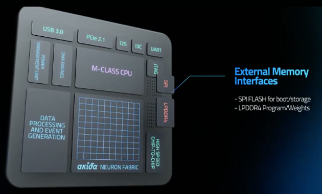
Secondly, while the tapeout of Akida1500 reference chip represents an important progression in the development of our IP portfolio and demonstrates our ability to customise our neuromorphic chip architecture to meet specific end-user requirements, the news itself has no immediate revenue or financial implications, and is therefore neither material nor price sensitive. Todays share price reaction to this news would appear to bare that point out. The threshold for these matters is "materiality" and its not always as clear cut as it seems from the outside.
As we've discussed in person, and I've discussed at countless retail investor engagements and in thousands of emails, we are adhering to the ASX Continuous Disclosure Guidelines and the Listing Rules. The decision to make an ASX announcement or a media release is discussed by our Board of Directors and our Executive Leadership Team and guided by the advice of our Company Secretary. I certainly have input into those discussions, but ultimately its a decision made by the CEO. We don't make these decisions lightly and we certainly do consider the expectations of shareholders and the market in those debates, but ultimately we are guided by the law and especially by the ASX, especially in regard to "ramping announcements". To have made an ASX announcement about the tape out of Akida1500 would have been a ramping announcement, as defined by the ASX.
I know that everyone has their own opinions on these matters, but opinions aren't facts. The fact is we are disclosing everything we are required to disclose and we are applying a conservative interpretation of the ASX continuous disclosure obligations, because we have run afoul of these obligations in the past and under previous management we ended up on an ASX watch list for repeated ramping announcement violations. We are not doing that again and we have sought advice from the ASX Compliance Team to satisfy ourselves that we are operating in compliance with their rules. This is not only good corporate governance but also a way of minimising our risk of regulatory intervention.
I know its probably a vain hope on my part that this note will end this discussion for good, but I hope it at least proves that we do listen to our shareholders and we are aware of their views and expectations. Please feel free to share this note on the BRN Discussion thread and I look forward to catching up with you at our next TSE-BRN Investor function in Perth. My best wishes to you and your lovely wife.
Regards
Tony Dawe


 . Will you all help me. I have $130 that I want to invest. I need a really cheap price. I’m worried that the share price bottomed out yesterday and I missed my opportunity.