Now look what you made me do:Cheers.
Is intriguing as you say though appears one thought last year was already to aim for 22nm and indicated AKD500 might be the implementation
Obviously mentioned 90nm as well which would tie in with NASA as you point out.
Akida spiking neural processor could head to FDSOI
Startup BrainChip Inc. has a road-map of larger and smaller SoC exemplars of its Akida spiking neural networking processing architecture and could go to fully-depleted silicon on insulator (FDSOI).www.eenewseurope.com
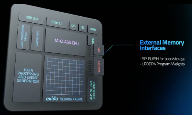
Anil Mankar, chief development officer, told eeNews Europe: “Chip production volume is just starting now. But you will see a lot of IP licensing going forward.” He added: “We are process agnostic.”
The near-term focus is supplying the Akida IP to 22nm although some customers may go back to 90nm process, Akida executives said.
Rob Telson, vice president of worldwide sales, said BrainChip is drawing up plans for smaller and larger versions of Akida under the names Akida500, Akida1500 and Akida2000. Some of these may well comply to a new generation of the Akida architecture – Akida 2.0 – due to arrive in 2022. It is thought Akida500 could be implemented in 22nm FDSOI manufacturing process, and serve as a demonstrator of the agnostic nature of the Akida architecture.

What is FDSOI anyway?
https://anysilicon.com/fdsoi/
FDSOI stands for Fully Depleted Silicon on Insulator. FDSOI is a planar process technology that provides an alternative solution to overcome some of the limitations of bulk CMOS technology at reduced silicon geometries and smaller nodes.
The FDSOI process has two distinct features. First starting with the substrate, an ultra-thin buried oxide layer is placed on the top of the base silicon. Second, a very thin silicon layer on top, creates the transistor channel. The FDSOI transistor is built above the buried-oxide layer. It has a raised source and drain and a very thin uniform channel under the gate. As the transistor channel layer is very thin, no channel doping is required, which makes the transistor fully depleted. The resulting FDSOI device is shown in the illustration in Fig. 1.1.
Fig. 1.1: FDSOI transistor
FDSOI is not only an alternative to continued CMOS scaling beyond 28nm node but also proves to be useful in improving the performances of older technology nodes when redeveloped using this process.
Two IDMs, STMicroelectronics and Renesas, also have their own FDSOI technology. STMicroelectronics adopted FD-SOI technology in 2012 and started several projects. STMicroelectronics is now using this technology for many diversified market applications. Renesas has a 65nm version of FDSOI called silicon-on-thin-BOx (SOTB), which targets ultra-low-power MCU markets. A partnership on FDSOI fabrication between ST and Samsung Foundry was announced in 2014. Today, two out of the world’s top foundries offer FDSOI technology fabrication. Samsung offers its 28nm and GF has its 22nm node fully developed for production. Many companies such as NXP, Sony, Mobileye started projects on FDSOI technology after the foundry system was in place. Today the IPs are well developed to make any sort of application possible. Both Samsung and GLOBAL FOUNDRIES are also developing its 18nm and 12nm nodes for future production, respectively. In Feb 2017, GF announced its plans to expand the capacity of its Fab 1 facility in Dresden due to market’s growing interest. In September 2017, Soitec announced to re-open its Singapore fab to meet increasing customer demand for wafers.
...
It provides improved speed and reduced power consumption* through a simple manufacturing process, so the power-performance-area-cost tradeoff is very good as compared to both bulk-CMOS and FinFet.
...
This technology is already supported by multiple foundries and IP solution providers for 28nm & 22 nm. The future roadmap 12nm is already in place and the process can be scaled down below 10 nm as well.
* Any more power reduction and Akida will become endothermal.
From "WayBack", this article appears to have been updated in November 2022.