Be patient with reading it leads to ReRAM.
"SEMICONDUCTOR MANUFACTURING
Of Frankenstein chips and computing memory
Chip development is moving away from the monolithic all-rounder - at least in part . For
AI , on the other hand, memory should no longer just store.
A reportfrom
Johannes Hiltscher published on July 13, 2022
View attachment 17339
Many individual silicon dies on a wafer: This almost certainly results in a working giant chip.
The term highly integrated circuit - also known as
Very Large Scale Integration (VLSI) - is getting a bit old. It dates back to the early days of semiconductor development, when 10,000 transistors on a chip was a revolution. The VLSI Symposium has had this name since 1981 - and it is still about the further development of semiconductor production. The 2022 Symposium was held in Honolulu from June 12-17.
The bandwidth of the submissions goes from the chip housing and the package to developments in production technology such as silicon photonics and semiconductors for quantum computers to new architectures for components such as memory. We have picked out some interesting topics from this year's VLSI Symposium and present them. The first is the so-called heterogeneous integration - it is found in everyday devices, is gaining importance and is becoming more and more complex.
AMD has shown the way with Ryzen and Epyc: Powerful processors can be assembled from several parts and are therefore cheaper to manufacture than a single, large die. Because the larger such a silicon plate is, the more likely it is defective somewhere. In addition, the individual dies can be manufactured in different processes - hence the name component "heterogeneous". With the current Ryzen 5000, for example,
the compute dies are manufactured with 7 nm, while the I/O die is made with 12 nm , which is cheaper.
Circuit boards have too few conductors that are too slow
Simply soldering the dies together on a circuit board, however, will foreseeably come up against limits for a number of reasons. For particularly powerful chips - GPUs and some particularly large FPGAs - special dies, so-called
silicon interposers , are used. The dies to be connected are mounted on them.
Since the interposers are also manufactured using semiconductor technology, particularly thin conductors and closely spaced contacts are possible. In this way, significantly more connections can be established between the individual dies - this means higher data rates. However, silicon interposers have a disadvantage: they are expensive. And in the end they have to be mounted on a circuit board, if only for the power supply. The interposer is completely useless for that.
Micrometer sized spring contacts
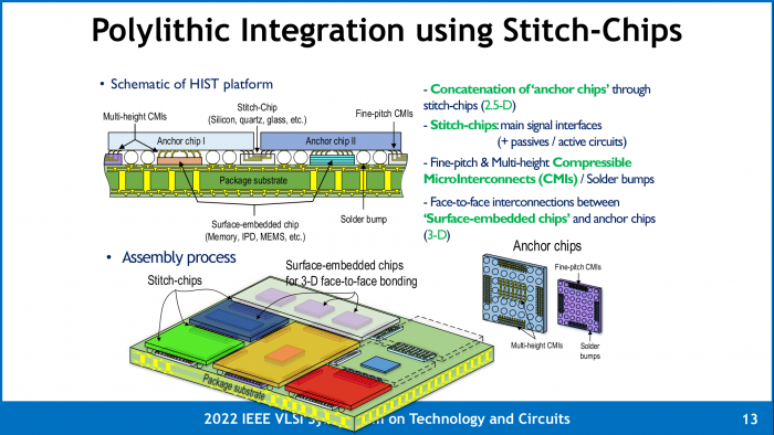
Muhannad Bakir from the Georgia Institute of Technology spoke about an alternative in which the die-to-die contacts are grouped and only connected using silicon interposers. Contacts that leave the package are soldered directly to its circuit board. The silicon interposers - or other chips that are mounted under the large dies - are mounted contacts up on the package. Since the distance to the dies below is smaller than to the package, solder balls of different sizes would be required when soldering.
-
- Inexpensive 3D chips with a large number of contacts and a wide variety of dies are conceivable with micro spring contacts. (Image: Georgia Institute of Technology)
Besides, soldering brings problems when the chip gets warm. Package and silicon expand at different rates, the tiny connections between the dies can break. So Bakir's research group developed tiny spring contacts. They are mounted on the silicon interposer, similar to the connection to the chip package with bonding wires. If the dies to be connected are soldered to the package, their contact surfaces press onto the spring contacts.
The resulting connection is as good as a soldered one. The flexibility of the contacts also compensates for differences in height; if the length of the spring contacts is adjusted, dies of different heights can even be contacted. This allows chips to be assembled from a wide variety of semiconductors - Frankenstein's monster made of silicon.
For the time being, however, silicon interposers remain state-of-the-art - and why not use an entire wafer as an interposer?
Wafer-Scale Integration
Puneet Gupta of the University of California, Los Angeles (UCLA) spoke about wafer-sized chips. The so-called wafer-scale integration currently uses Cerebras for its AI processors. They consist of a
complete wafer with hundreds of thousands of individual computing cores . A connection network (interconnect) is also integrated, which enables communication between the cores.
Manufacturing all processors in the same piece of silicon has a number of advantages. There are no transitions to other materials as with soldering on a circuit board (substrate). This allows higher signal frequencies. In addition, with semiconductor manufacturing - as with interposers - conductors can be packed much more closely. In this way, significantly more connections can be implemented between the processors.
With many lines, high data rates can be transmitted without serial interfaces, which saves chip area and energy and reduces latency. There's only one catch: Some of the individual processors will be defective. In normal chip production, they would be sorted out, but if the entire wafer is used as a huge chip, that doesn't work. Then logic must be built in to deal with the defects.
A huge interposer
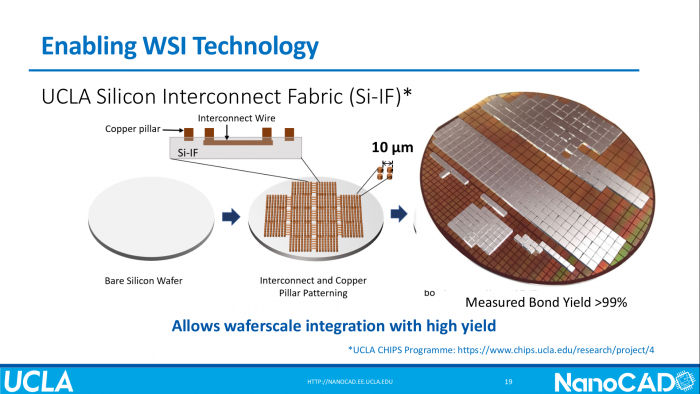
The problem can be avoided by manufacturing the logic and interconnect on different wafers. The logic wafers are regularly tested, sawed into dies and faulty ones sorted out. They are then mounted on the interconnect wafer. This has the additional advantage that dies from different manufacturing processes can be combined. Although fewer lines can be integrated than in a monolithic chip, the approach is still far superior to a printed circuit board.
-
- Structure of a waferscale interposer (Image: University of California)
With the interposer approach, only simple conductors and small copper columns are produced on the interconnect wafer. There are hardly any defects, since the structures are huge compared to the transistors and smallest conductors of current manufacturing processes. The copper pillars are 10 μm apart - by the way, they make contact with the logic chips, which are attached using
thermocompression bonding . The process was originally
used in flip chip assembly , but is also used at HBM.
A wafer full of problems
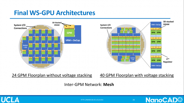
A whole wafer full of computing units, however, causes further problems even if it has been successfully manufactured. The many dies also require a lot of energy, and it first has to get to them in the form of electricity - and then away again in the form of heat. Gupta illustrated this on a waferscale chip with GPUs. Theoretically, 72 GPU dies, each with two associated HBM stacks, would fit on a 300 mm wafer.
However, the practical maximum is 40 GPUs, and even that only with two-stage regulation of the supply voltage. Since each GPU consumes 270 W of power together with the HBM stacks, at least 10.8 kW must be supplied in the form of electrical power and dissipated again as heat. Conversion losses are not yet taken into account. With Cerebra's Wafer Scale Engine 2 it's even 20 kW -
they can only be cooled with water .
-
- With waferscale integration, UCLA has realized a huge GPU. The design of the power supply (VRMs, Voltage Regulator Modules) had to be adapted for this. (Image: University of California
Waferscale integration aims to increase computer performance through faster connections. In some cases, however, it can make sense to rethink the architecture itself.
Computing memory
AI applications in particular have quite an efficiency problem: neural networks
like Megatron have hundreds of billions of parameters - even larger AIs are only a matter of time. Even if only one byte is used per parameter (e.g. Int8), that's hundreds of gigabytes - and they have to be moved from memory to processors on a regular basis.
However, they are only used for a few arithmetic operations there. This not only means latency due to memory access, but also requires a lot of energy. In the RAM chip, the data is read from the memory array into a buffer and then transferred to the processor via the mainboard (or an interposer). There they are buffered several times until they end up in a register and the calculation takes place. The result must then return on the same path.
One possible solution to this efficiency disaster is called compute in memory (CIM, not to be confused with in-memory computing for databases). The memory itself becomes the computer, which saves electrical power, since only the results leave the memory. In addition, the calculations take less time due to the direct access to the storage array.
The idea has been around for a while, but...
The idea isn't new, one of the most famous projects, the University of Berkeley's
Intelligent RAM (IRAM) , started in 1998 (led by
David Patterson , one of the fathers of RISC design). So far, the concept has not caught on, the niche was perhaps too small. But it could be given a new chance for neural networks.
-
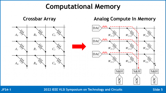
- This is how ReRAM calculates: The individual memory cells, implemented with adjustable resistors, record the weight coefficients of a neuron, the digital-to-analog converters (DACs) enter the activations. The columns add up the individual currents, and an analog-to-digital converter (ADC) generates a digital output. (Image: University of Michigan)
Instead of integrating a CPU into the memory chip, as is the case with IRAM, the memory chip itself becomes a computer - an analog computer at that. This is made possible by resistive RAM, in which the memory cells do not store an electrical charge, but rather a resistance. You can even set different values. The secret of the analog computer lies in the resistances: If a voltage is applied, the current is the quotient of voltage and resistance - i.e. a division. If several resistors are connected in parallel, the currents add up.
These two operations are sufficient for a neural network, at least for inferencing: In each neuron, input values are multiplied by a weight (the inverse of division) and the results are summed.
Justin Correll presented an implementation from the University of Michigan at the VLSI Symposium. It clearly sets itself apart from older, also ReRAM-based publications through higher resolution for weighting and input values as well as a larger number of weighting coefficients. In terms of efficiency, however, with the achieved 20.7 TOPS/W (20.7 trillion arithmetic operations per watt), it remains far behind the 2,900 TOPS/W of an
SRAM-based chip presented in 2020 .
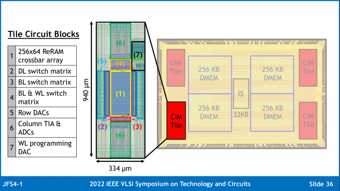
There is also room for improvement in terms of size: the experimental memory can only hold 64 neurons, each with 256 4-bit weight coefficients. So for Megatron it has to be written to often, but it is also not intended as a replacement for normal DRAM. Rather, the ReRAM exists as a computing unit parallel to the normal DRAM. In the test chip, which was manufactured in cooperation with Applied Materials, a CIM block with 8 Kbytes of capacity occupies about a third of the area of a 256 Kbyte DRAM. One reason for this is the required digital-to-analog and analog-to-digital converters, which serve as an interface between the analog CIM module and a digital processor.
-
- Four CIM blocks with associated DRAM are implemented in the ReRAM test chip. In the CIM modules, DACs and ADCs take up a lot of space. (Image: University of Michigan)
And when is all this coming?
With the CIM presented last, it is not yet foreseeable that it will end up in products. However, interest in these and other analog computers has increased again with the increasing importance of AI. Here they are superior to a classic processor in terms of efficiency, especially in mobile, battery-powered devices.
When it comes to packaging, on the other hand, there is considerable movement: the trend is clearly towards more dies per package. In addition - as with Frankenstein's monster - more and more different semiconductors are combined. The stronger integration is used both in high-performance chips such as GPUs and in efficiency-optimized SoCs such as smartphones. TSMC, for example
, has built a new factory for increasingly complex packaging methods. This increases the possibilities for chip designers. The VLSI Symposium showed that there is no shortage of ideas."
https://www.golem.de/news/halbleite...ps-und-rechnendem-speicher-2207-166713-3.html

