I often go back to the Renesas tape out Ann to reread its context.
Key question for me is the following couple of paragraphs plus the common theme we are now seeing with 22nm both through Renesas in Dec and by BRN with GF...
They way I read the below is that Renesas have had someone come to them and request the tape out and device but open to interpretation I guess.
The other part is that Renesas will let the mkt decide on something like this as to the uptake and then decide if they will bring in house for control or just continue external 3rd parties to run with it.
Renesas is taping out a chip using Brainchip's spiking neural network (SNN) technology and expanding internal and foundry capacity

www.eenewseurope.com
“Now you have accelerators for driving AI with neural processing units rather than a dual core CPU. We are working
with a third party taping out a device in December on 22nm CMOS,” said Chittipeddi.
The take up of the technology depends on the market adoption, he says.
“We want to see where the market reception is the highest,
that is what determines whether we bring things in house or through a third party.”
Now...another recent article I was just reading is about GF and quite interesting group of names discussed including BRN.
Be nice to get in with Purdue as well. Intel in there and our own K Carlson published papers on STDP in 2011 via Purdue.
In a Series of Agreements, GlobalFoundries Buoys Chip Supply From Home
3 days ago by
Biljana Ognenova
Tracking the goals of the CHIPS+ Act, GlobalFoundries is strengthening the U.S. semiconductor ecosystem with several partnerships and acquisitions.
The U.S. semiconductor manufacturing industry is beginning to reap the benefits of the
CHIPS+ Act passed in July 2022. In a series of collaborations and acquisitions, GlobalFoundries (GF) is progressing toward one of the act's goals: to strengthen a U.S.-based semiconductor supply chain and reduce dependence on Asia-based manufacturers. Throughout the chip shortage, GF claims it has remained profitable by steadying productivity, containing cost, differentiating products, and doubling down on supply chain security.
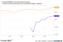
A comparison of GF's and TSMC's EBIT margins. Image courtesy of Seeking Alpha
GlobalFoundries attributes its upward profitability to its strategic approach to chipmaking and its local partnership with key industry sectors, including automotive, memory, and computing as well as education.
GlobalFoundries Partners With GM, Renesas, and Purdue
In a major win for GF in the automotive sector, the foundry
signed an agreement with GM on Feb. 9, 2023, to dedicate a manufacturing corridor at GF's upstate New York facility for GM’s key chip suppliers.
GF also secured more production capacity by
acquiring Renesas' NVM resistive RAM technology. Specifically, GF now owns Renesas' proprietary Conductive Bridging Random Access Memory (CBRAM) technology, a low-power memory solution built for home and industrial IoT and mobile devices.
GF has secured wins in the education and R&D sector as well,
partnering with Purdue University on a semiconductor education program. Purdue was among the first institutions to use the funds from the CHIPS+ Act to finalize a
university-level semiconductor program. Now, with this new collaboration, Purdue's staff and students will use GlobalFoundries' facility and resources to create innovative, interdisciplinary solutions for advanced semiconductors and microelectronics. The partnership between GF and Purdue will provide next-generation professionals with hands-on expertise overseen at GF Lab.
GF Supports Next-gen Vision and Computing Technologies
GF is also championing the computing sector, namely with BrainChip's Akida neuromorphic chip
built on 22 nm fully depleted silicon-on-insulator (FD-SOI) technology.
Akida architecture. Image courtesy of BrainChip
BrainChip is the world’s first company to develop ultra-low-power, event-based, neuromorphic AI IP to be used for always-on sensor applications. The AKD1500 chip was built on GF’s low-leakage FD SOI platform, promising an array of applications that don't overload the CPU.
Vision sensor specialist Oculi also recently announced
a strategic partnership with GF, commissioning the foundry to manufacture its single-chip, intelligent software-defined vision sensor. The new sensor will be based on GF’s 55LPx, a platform that supports RF, ultra-low power, embedded NVM, and high-voltage BCDLite (a process technology).
Expanding U.S.-based Semiconductor Production
While GlobalFoundries relies on five-year agreements to ship chips from storage facilities in Dresden and Singapore, the foundry also plans to expand three U.S. locations, including one in Vermont and two in New York. Specifically, GF is broadening the scope of existing facilities to make 12 nm, 28 nm, and 40 nm chips rather than going back to the drawing board and investing in new technologies to compete with
TSMC’s advanced 3 nm – 5 nm chips.
GlobalFoundries' headquarters in Malta, New York. Image (modified) courtesy of GlobalFoundries
GF has increased existing domestic manufacturing capacity in another way, too. The company has invested in gallium nitride (GaN) RF chips, a wide-band semiconductor technology that outperforms silicon in terms of thermal resistance and durability. GF's development of GaN devices at its Essex Junction, Vermont, facility would have been impossible without a $30 million government grant to shorten the time to market for the GaN RF technology.
A GF facility in upstate New York is also getting a boost—this time, from collaborating with Qualcomm. The U.S. mobile chipmaker has previously agreed to spend $4.2 billion on chips made by GF for Qualcomm's 5G transceivers, automotive products, and IoT connectivity.
I also posted not long ago about NASA and the 22nm FDSOI requirements plus that there wrote the same chip was often used for automotive.
Well, just seen this older solicitation with some further support for the 22nm. Ends mid this year.

www.sbir.gov
Radiation Tolerant Standard Cell Library in a 22nm FDSOI CMOS Process
Award Information
Agency:National Aeronautics and Space Administration
Branch:N/A
Contract:80NSSC21C0516
Agency Tracking Number:205369
Amount:$759,984.00
Phase

hase II
Program:SBIR
Solicitation Topic Code:Z2
Solicitation Number:SBIR_20_P2
Timeline
Solicitation Year:2020
Award Year:2021
Award Start Date (Proposal Award Date):2021-07-27
Award End Date (Contract End Date):2023-07-26
Small Business Information
ALPHACORE INC
304 South Rockford Drive
Tempe, AZ 85281-0000
United States
NASA is seeking radiation tolerant standard cell libraries for processes below 28nm that are suitable for NASA missions in the natural space environment. As a response, Alphacore proposes to develop for NASA an innovative library of radiation-hardened (rad-hard) standard cells implemented in the GlobalFoundries (GF) 22nm fully depleted silicon on insulator (FDSOI) CMOS fabrication process (GF 22FDX).nbsp;Alphacore has been able to have the first version of the radiation tolerant library important cells already designed by the end of the Phase I program. The Phase I program provided an excellent basis for the Phase II program in which an extended, innovative radiation-tolerant standard cell library will be designed, fabricated, and tested. The library elements will be taped in the middle of the Phase II program and knowing the fabrication time for chips in the 22FDX program is 2.5 - 3 months, the evaluations can start approximately 3.5 months after the tapeout date. The elements will be tested for functionality, circuit performance and radiation hardness, including both single event effects (SEE) and total ionizing dose (TID).During Phase II, Alphacore will not only support CMOS IP development for the most harsh NASA mission environments (low temperatures and high radiation), but also covering critical immediate needs in other areas such as the High-Performance Spaceflight Computing (HPSC) Chiplet, a radiation-hardened multi-core processor. NASA also will be developing single board computer based on this chiplet. These components are supposed to bring NASA (and DoD) a two orders of magnitude improvement in their space computing capabilities.