Some slightly dated (well, last few months anyway) articles / news on Intel & SiFive over next couple posts.
Obviously, we know pretty much all the content but still think all worth a skim through at least IMO as can see various connections and where we can fit as well.
I read earlier FF reminding us of VCIX implementation on the X280 & WikiChip Fuse in Sept gives us a better insight.
SiFive introduces a new high-performance coprocessor interface targeting custom accelerators; scores design wins from Google, NASA.

fuse.wikichip.org
SiFive Introduces A New Coprocessor Interface, Targets Custom Accelerators
September 20, 2022 David Schor AI,
AI Hardware Summit,
Linley Processor Conference,
neural processors,
SiFive,
Vector Coprocessor Interface Extension (VCIX)
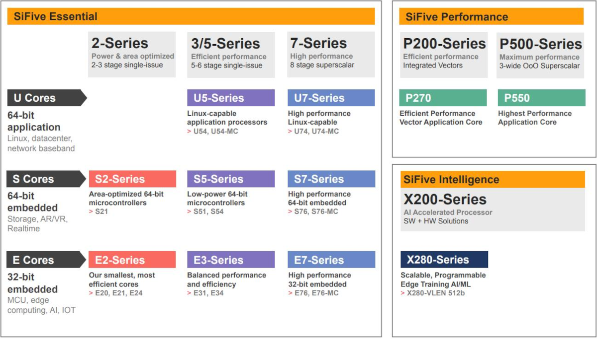
Last year SiFive introduced the Intelligence X280 processor, part of a new category of RISC-V processors for SiFive that aims at assisting AI and machine learning workloads.
Launched under the new family of processors called SiFive Intelligence, the X280 is the first core to cater to AI acceleration. At a high level, the X280 builds on top of their silicon-proven
U7-series high-performance (Linux-capable) core. SiFive’s Intelligence X280 is somewhat of a unique processor from SiFive. Targetting ML workloads, its main feature point is both the new RISC-V Vector (RVV) Extension as well as SiFive Intelligence Extensions – the company’s own RISC-V custom-extension for handling ML workloads which includes fixed-point data types from 8-bits to 64-bits as well as 16-64 bit FP and the BFloat16 data type. On the RVV extension side, the X280 supports 512-bit vector register lengths, allowing variable length operations up to 512-bits.

As we mentioned earlier, the X280 builds on SiFive’s successful
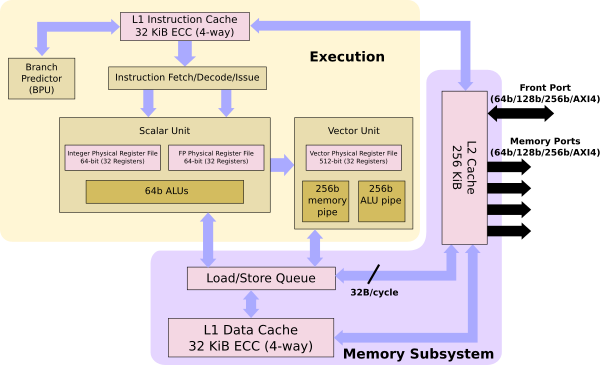
U7-series core. This is a 64-bit RISC-V core supporting the RV64GCV ISA and extensions. It is an 8-stage dual-issue in-order pipeline. Each core features 32-KiB private L1 data and instruction caches as well as a private L2 cache.

The RISC-V Vector extension is a variable length instruction set. For the X280, the core utilizes a 256b pipeline. In other words, both the vector ALU and load/store architecture data width is 256-bit, doing two operations per 512-bit register data. In addition to the vector extension, SiFive added the “Intelligence Extensions” part of the RISC-V custom extensions ISA support. SiFive didn’t go into any details as to what those extensions entail but did note that compared to the standard RISC-V Vector ISA, the Intelligence Extensions provide a 4-6x performance improvement in int8 (matmul) and bf16 operations.
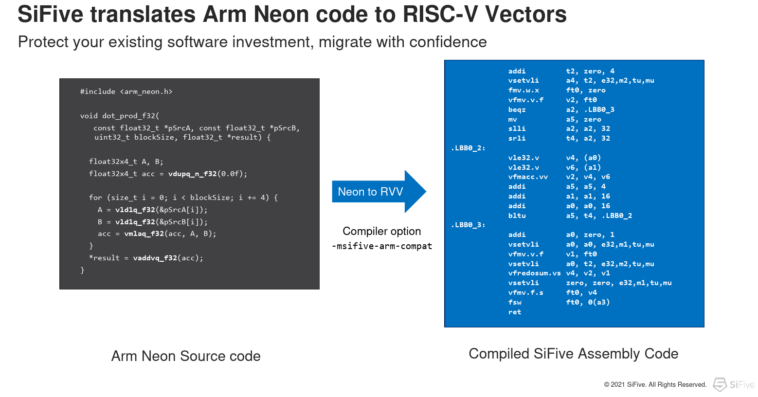
One of the interesting things that SiFive has done is add that capability for automatic translations of Arm Neon vector code into RISC-V Vectors directly into their compiler. And while it may not produce the most optimal code, it’s a way to quickly and accurately move on Arm Neon code directly to SiFive’s RISC-V code. At last year’s Linley Processor Conference, According to Chris Lattner at Last year’s, SiFive’s then President of Engineering & Product group noted that SiFive itself has been using this feature to port a large number of software packages.

Each of the X280 cores goes into an X280 Core Complex which supports up to a quad-core coherent multi-core cluster configuration. The core cluster can be fully scaled up in a configuration that consists of up to 4 clusters for a total of 16 cores. A system-level L3 cache made of 1 MiB banks (up to 8 MiB) is also supported. The system supports a rich number of ports for I/O and communication with other important sub-system components via the system matrix.
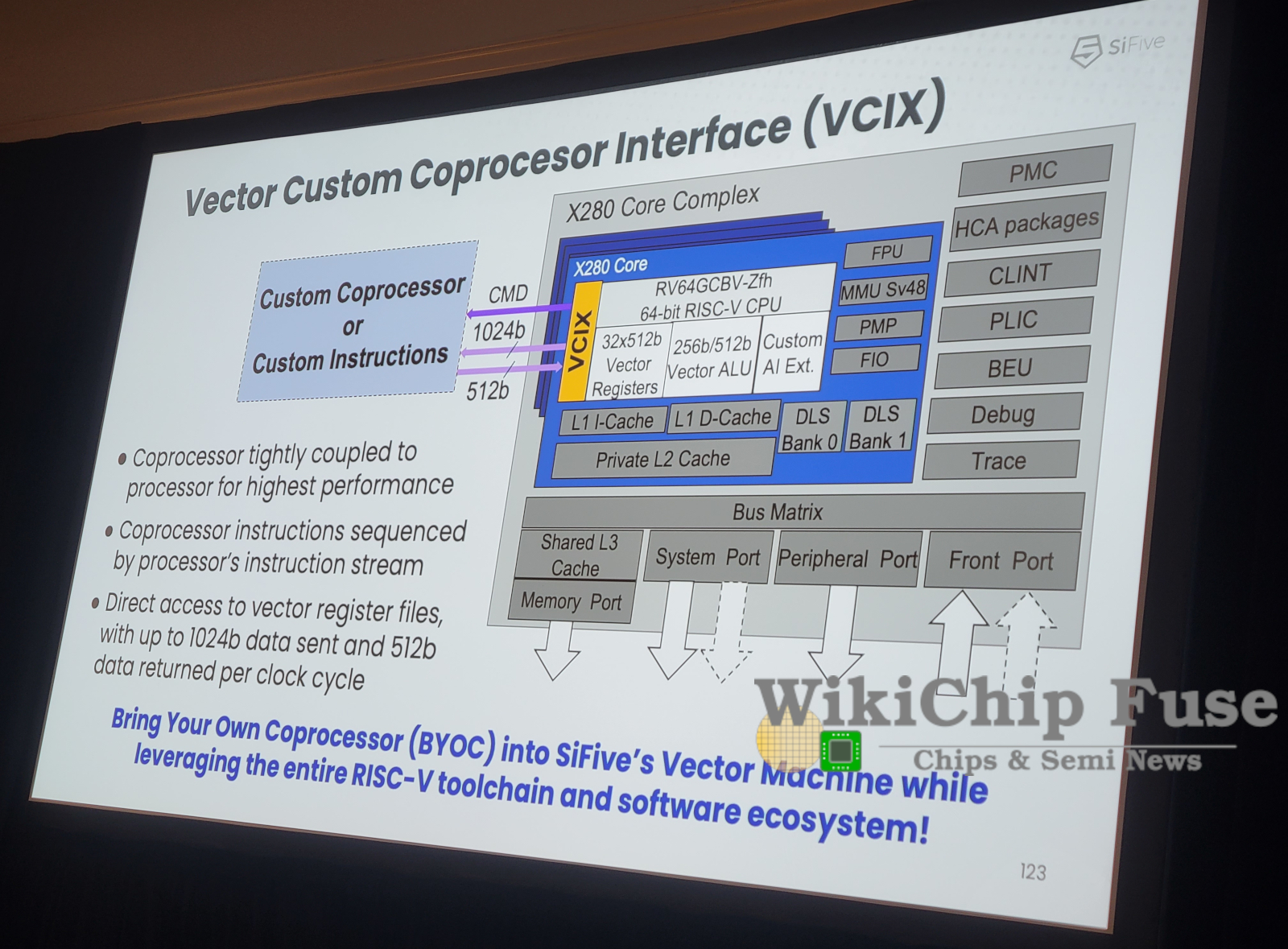
Vector Coprocessor Interface Extension (VCIX)
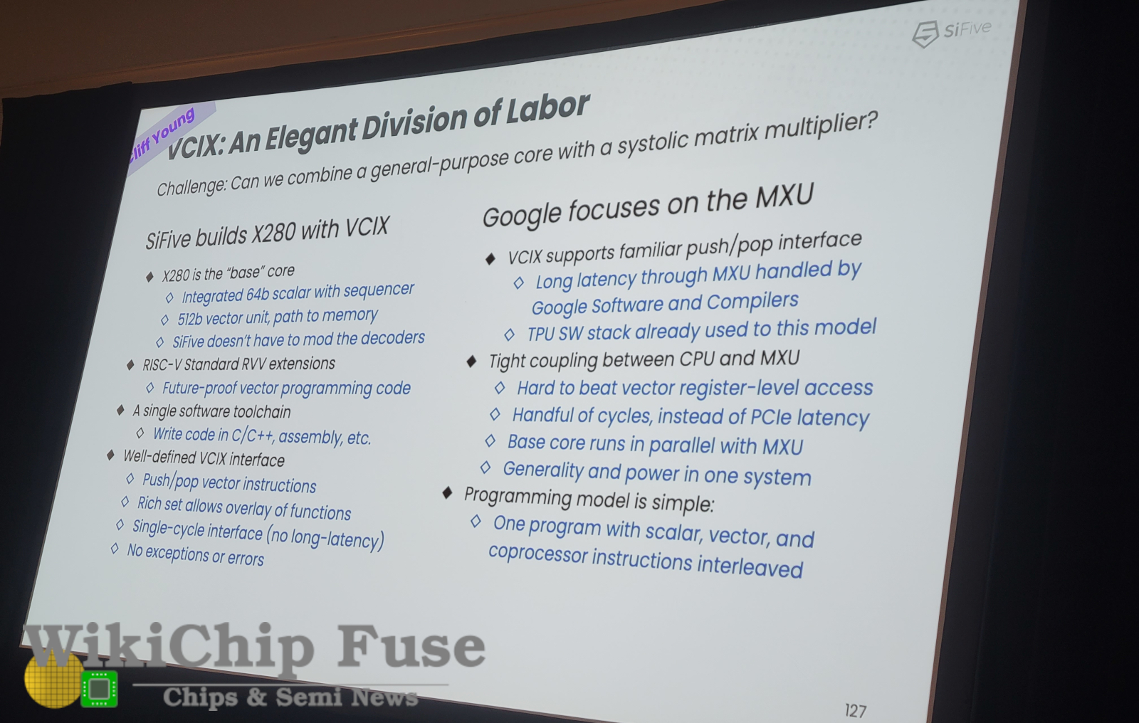
At the 2022 AI Hardware Summit, Krste Asanovic SiFive Co-Founder and Chief Architect introduced a new Vector Coprocessor Interface Extension (VCIX).

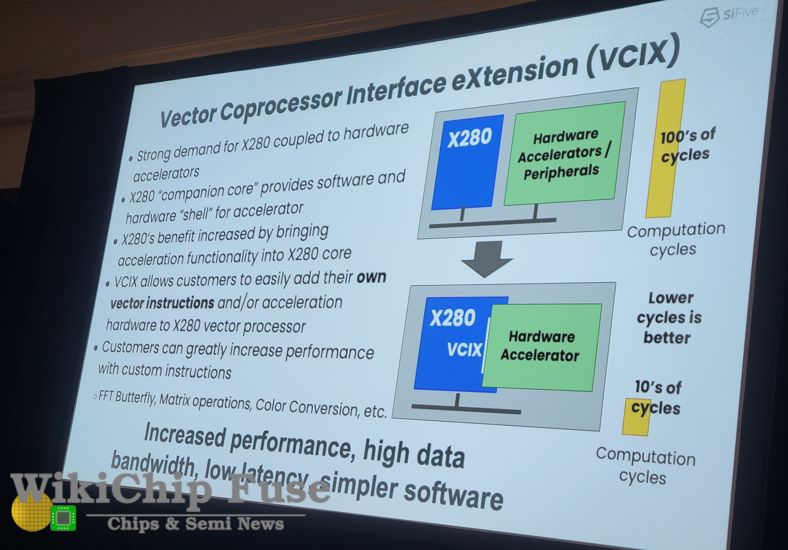
As customer evaluation of the X280 went underway, SiFive say it started noticing new potential usage trends for the core. One such usage is not as the primary ML accelerator, but rather as a snappy side coprocessor/control processor with ML acceleration functionality. In other words, SiFive says it has noticed that companies were considering the X280 as a replacement coprocessor and control processor for their main SoC. Instead of rolling out their own sequencers and other controllers, the X280 proved a good potential replacement.
To assist customers with such applications, SiFive developed the new Vector Coprocessor Interface Extension (VCIX, pronounced “Vee-Six”). VCIX allows for tight coupling between the customer’s SoC/accelerator and the X280. For example, consider a hardware AI startup with a novel way of processing neural networks or one that has designed a very large computational engine. Instead of designing a custom sequencer or control unit, they can simply use the X280 as a drop-in replacement. With VCIX, they are given direct connections to the X280. The interface includes direct access into the vector unit and memory units as well as the instruction stream, allowing an external circuit to utilize the vector pipeline as well as directly access the caches and vector register file.
The capabilities of essentially modifying the X280 core are far beyond anything you can get from someone like Arm. In theory, you could have an accelerator processing its own custom instructions by doing operations on its own side and sending various tasks to the X280 (as a standard RISC-V operation) or directly execute various operations on the X280 vector unit by going directly to that unit. Alternatively, the VCIX interface can work backward by allowing for custom execution engines to be connected to X280 for various custom applications (e.g., FFTs, image signal processing, Matrix operations). That engine would then operate as if they are part of the X280, operating in and out of the X280’s own vector register file. In other words, VCIX essentially allows you to much better customize the X280 core with custom instructions and custom operations on top of a fully working RISC-V core capable of booting full Linux and supporting virtualization.

The VCIX is a high-performance direct-coupling interface to the X280 and its instruction stream. To that end, Asanovic noted that on the X280 with the new VCIX interface, the X280 is capable of sending 1,024 bits over onto the accelerator/external component each cycle and retrieving 512 bits per cycle, every cycle sustained over the VCIX interface.
SiFive says that utilizing their Vector Coprocessor Interface Extension, various accesses and operations from outside can now be done in as low as single-digit cycles or 10s of cycles, instead of 100s of cycles from the normal cluster bus interfaces or memory mapped interfaces. Extremely low-cycle latency is important for developing computational circuits that are highly integrated with the X280.

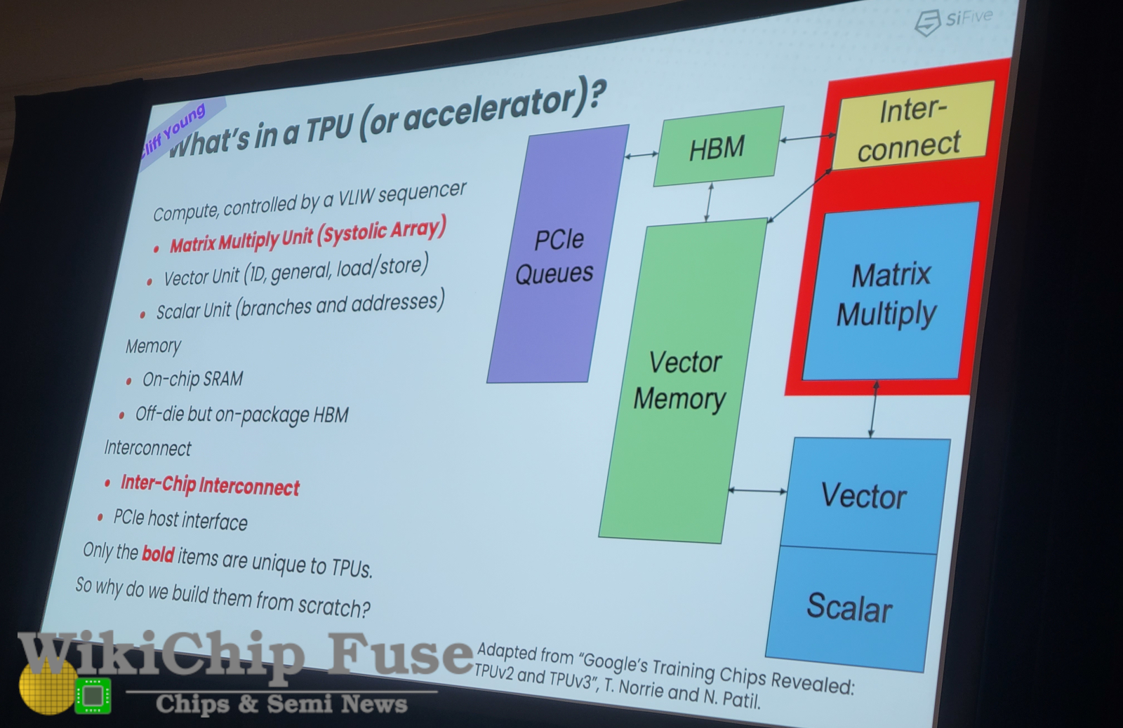
Google Accelerators
Cliff Young, Google TPU Architect, and MLPerf Co-Founder was also part of the SiFive announcement. As we’ve seen from other Google accelerators, their hardware team always looks to eliminate redundant work by utilizing off-the-shelf solutions if it doesn’t add any real value to design it themselves in-house.

For their own TPU accelerators, beyond the inter-chip interconnect and their highly-refined Matrix Multiply Unit (MXU) which utilizes a systolic array, much of everything else is rather generic and not particularly unique to their chip. Young noted that when they started 9 years ago, they essentially built much of this from scratch, saying “scalar and vector technologies are relatively well-understood. Krste is one of the pioneers in the vector computing areas and has built beautiful machines that way. But should Google duplicate what Krste has already been doing? Should we be reinventing the wheel along with the Matrix Multiply and the interconnect we already have? We’d be much happier if the answer was ‘no’. If we can focus on the stuff that we do great and we can also reuse a general-purpose processor with a general-purpose software stack and integrate that into our future accelerators.” Young added, “the promise of VCIX is to get our accelerators and our general-purpose cores closer together; not far apart across something like a PCIe interface with 1000s of cycles of delay but right next to each other with just a few 100s of cycles through the on-chip path and down to 10s of cycles through direct vector register access.”
The SiFive-Google partnership announcement is one of several public announcements that took place over the past year. Last year SiFive announced that AI chip startup Tenstorrent will also make use of the X280 processor in its next-generation AI training and inference processors. Earlier this month, NASA announced that it has selected SiFive’s X280 cores for its next-generation High-Performance Spaceflight Computing (HPSC) processor. HPSC will utilize an 8-core X280 cluster along with 4 additional SiFive RISC-V cores to “deliver 100x the computational capability of today’s space computers”.


")