Fullmoonfever
Top 20
Just found an article from yesterday which outlines Oculi and GF producing 3 chips but the first is using their 55LPx whereas AKD1500 is in 22FDX.My reason for the question is the paragraph below that was written in the Akida 1500 tape out article:
"The tape-out was completed using GlobalFoundries’ 22nm fully depleted silicon-on-insulator (FD-SOI) technology and is being described as a milestone in validating BrainChip’s IP across different processes and foundries, providing its partners with varied global manufacturing options."
The Brainchip/Global Foudries tape out was announced on 29th Jan 2023.
Two days ago, Oculi, whom Brainchip is working with, announced that they are using Global Foundries to help them produce their latest chip (did the Akida 1500 tape out on Global Foudries technology give them what they needed to go ahead with their own GF chip?):
Oculi say this about their future chip:
"Oculi’s new vision is ideal for edge applications such as always-on gesture/face/people tracking and low-latency eye tracking, while alternative solutions are too slow, big, and power inefficient. GF is an excellent partner to enable us to quickly get our product to our customers."
Maybe @Diogenese can impart some wisdom as to the outcome here?
Get the feeling maybe no crossover as yet?
Maybe the AKD1500 will be testing etc for the stated next iterations of the SPU.

Smart vision startup Oculi turns to GF for next chips
Oculi, a fabless company seeking to add intelligence to image sensors at the pixel level, has partnered with chipmaker GlobalFoundries Inc.
 www.eenewseurope.com
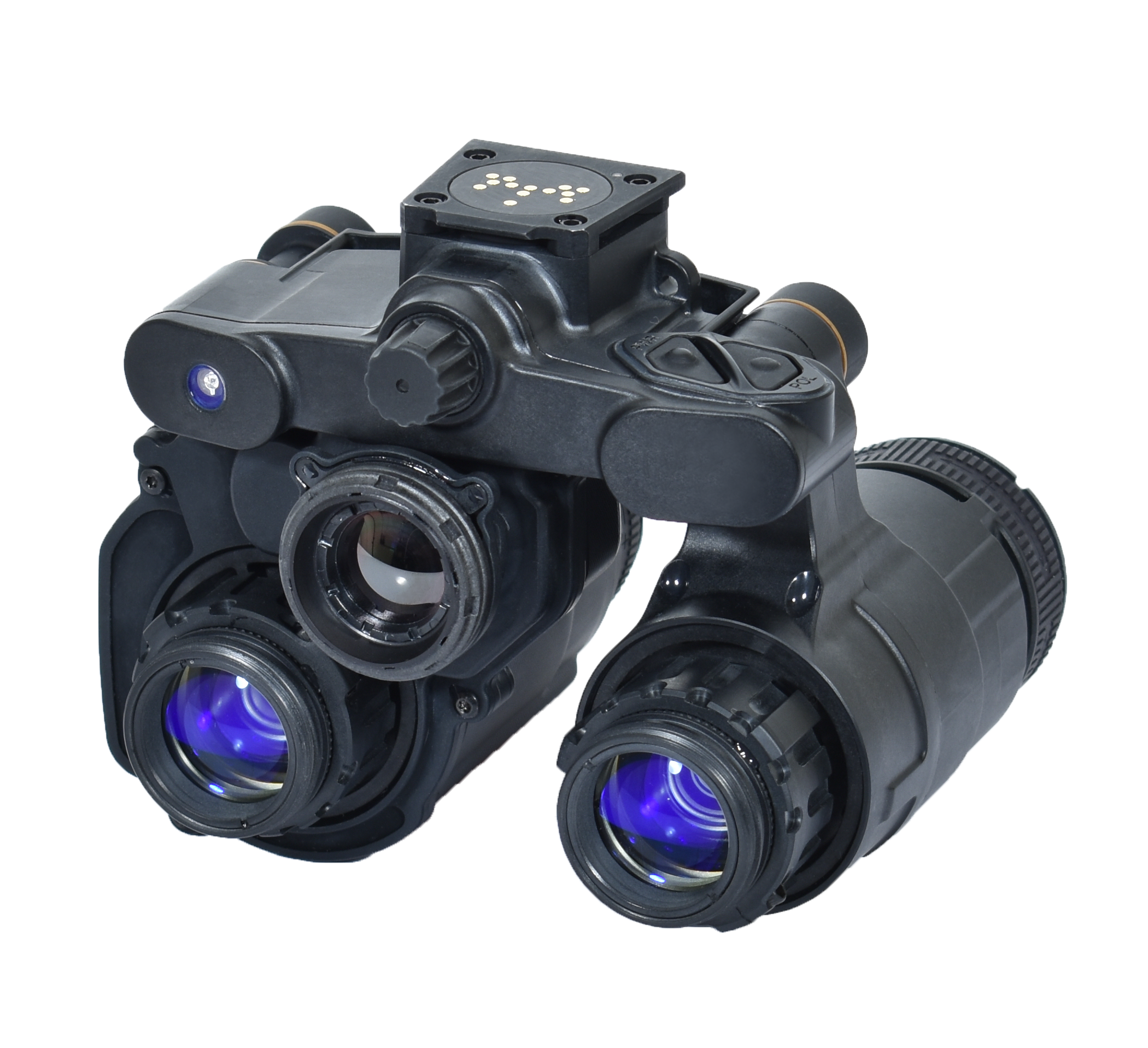
Under the agreement GlobalFoundries will manufacture the SPU (sensing and processing unit) S12 software-defined vision sensor in its 55LPx manufacturing process. The chip is intended to be used for applications in smart devices and homes, industrial, IoT, automotive markets and wearables including AR/VR.
The SPU S12 will be the first of three sensors to follow on from the SPU S11 which Oculi offers on a series of PCB-based platforms.
For outline of GF chips.

Industrial IoT | GlobalFoundries
Bring forth Industry 4.0 with GF From agriculture to manufacturing, intelligent connectivity and AI are leading the way in the […]
Industrial MCUs using 22FDX® with eNVM
GlobalFoundries® (GF®) 22FDX® solutions, featuring low power, adaptive body bias, analog scaling and robust eNVM capabilities, enable integrated, area and power-optimized industrial MCUs. Solution options include eMRAM, low-cost charge trap technology (CTT) and CB-RAM embedded memory for faster TTM and wakeup times.
Pumped up, power-efficient performance
22FDX® offers best-in-class performance at the industry’s lowest operating voltage for bulk CMOS technologies (0.4 V) and 1 pA/µm for ultra-low standby leakage. It features an eMRAM NVM with >100x lower write power* that enables frequent, power-saving shutdowns to help designers extend battery life while boosting processing capability.
More function, in less space
22FDX® solutions enable designers to develop RF front-end modules (FEMs) with outstanding PA efficiency, LNA noise figure, and switch insertion loss benefits. These FEMs, baseband and eMRAM elements can be integrated into a single IIoT SoC that helps designers combine the features needed to meet goals, while significantly reducing overall area—and costs.
Design, made simple
The 22FDX® portfolio of silicon-proven, MCU-optimized IP, along with a broad range of services and solutions available through GF and the FDXcelerator™ partner program, can help designers reduce development time and have confidence in first-time-right results in hardware.
Industrial MCUs using 55LPX and 40LP with eNVM and 28SLP-ESF3
GlobalFoundries® (GF®) 55LPX and 40LP with eNVM and 28SLP-ESF3, built on bulk CMOS platforms, are optimized for range of power-performance and cost-sensitive MCU applications, including automotive, baseband SoCs, mobile multimedia, digital TVs/STBs, IoT and industrial. The solutions enable designers to leverage logic, analog, RF, ULP SRAM/logic combinations, high-K metal gate technology and high reliability, along with on-board memory (eNVM) for faster wakeup times, reduced system cost and improved security:
55LPx features high reliability (automotive-grade IP) and high-density, low-power SRAM
GF’s 40LP is the only 40 nm automotive grade 0 offering in the industry
28SLP is optimized for power, performance and die cost, when flexible mixed-technology options for RF and ultra-low power are required
ESF3 eFlash adds robust quality and reliability, offering zero failure rates in harsh temperature conditions
High voltage? No problem.
55LPx solutions are excellent fits for analog and power devices operating at 30 V and beyond; it is optimized for integrated analog, power and mixed-signal applications such as PMICs for mobile devices, audio amplifiers and applications requiring dense digital, analog and power elements.


 Breaking news!