Just over a year ago, I spotted an intriguing comment by Alf Kuchenbuch under a STEMIX.TECH LinkedIn post. The founders of this Romanian startup “specializing in AI-centric hardware and software products” had previously worked for CyberSwarm, a neuromorphic startup with roots and an R&D centre in Romania as well, but headquartered in San Mateo, CA.
View attachment 88970
View attachment 88973
(…)
View attachment 88974
While we never heard anything concrete with regards to an actual collaboration between BrainChip and STEMIX.TECH in the ensuing months, I did notice a number of LinkedIn ‘likes’ being exchanged, including this recent one: Their CTO Ionuț Moldovanu gave Alf Kuchenbuch’s Edge AI Milan 2025 post a

, in which our VP of Sales, EMEA had mentioned “validating our approach with Akida2 with TENNs, which we will start rolling out for evaluation in summer 2025”:
View attachment 88975
So it appears our companies are still interested in each other, if not already secretly an item.
Although the AI toy project sounded pretty advanced in development at the time (“We’re about to launch…”), STEMIX.TECH never again referred to it on LinkedIn.
Is the Bucharest-based startup still working on it in secrecy?
Or have they meanwhile shelved that project, which would actually be somewhat surprising, given what their CTO stated in this video uploaded to YouTube on 17 June 2024, less than a month before Alf Kuchenbuch made the above comment, whose content suggested they had already been in contact for some time.
“STEMIX.TECH D1 demo video - Voice AI development kit - Use the full power of LLM with our low power development board”:
From 3 min onwards, Ionuț Moldovanu says “Basically you could run a lot of other apps, like voice-to-voice - we’re gonna do a demo with that one as well. You could also tie sensors to it, so the generation could be made accordingly to what the sensors see, sensor values [?].
You can embed it in wearables, you can embed it in industrial equipment, in toys. Actually toys are one of our best choices right now for integrating this device, because smart toys with connections to LLM could be really interactive and engaging for users.”
I pointed out at the time that the envisaged smart toy appeared to be conceptualised as cloud-based, which made me wonder how our company would fit into this, since we keep on spruiking the benefits of privacy and security thanks to on-device processing without having to send data to and from the cloud. Remember, we’re talking about an electronic children’s toy here, where data protection should be of paramount importance!
Also, our potential partner was a yet unknown Romanian startup. It seemed implausible that they would have the budget to take out a regular IP license with us, although our business model had evolved into just that - IP licensing... That’s why I wrote at the time: “So is this possibly a case of a collaboration involving a potential software license of TENNs only?! After all, you don’t necessarily need Akida for running TENNs!”
Fast forward a year and see our BrainChip team buzzing with excitement about Akida GenAI and LLMs on the Edge. This made me revisit that July 2024 STEMIX.TECH post and speculate whether the reason why the smart toy hasn’t yet been launched may possibly have to do with our company convincing the STEMIX.TECH team at the time to shelve their original concept of utilising LLM cloud models, and instead offer to work with them on “LLMs on the Edge” in the true sense of the word: “Small Large Language Models” that can fit on a chip inside the toy and function without any internet connection, hence keeping conversations between children and their AI toys private and safe, all within the family’s four walls.
Is BrainChip possibly working with STEMIX.TECH in the form of a joint partnership (which would circumvent any upfront licence fee) to demonstrate what is possible with regards to LLMs at the Edge?

As I said, all this is pure speculation only. Maybe the project simply got shelved - be it temporarily or indefinitely.
Shortly after the LinkedIn post about the AI toy, STEMIX.TECH announced a partnership with Butonul Roșu - Niciodată Singur (
https://butonulrosu.ro/, Butonul Roșu meaning “Red Button”) on the development of an “LTE-M SOS enabled bracelet or keychain focused on safety and health monitoring”.
What piqued my interest about this device - given I was aware of BrainChip’s prior intention of working on another project with STEMIX-TECH - is the sentence “The IoT-LLM technology we are developing will be part of the next wave of energy efficient, AI integrated hardware and software products. It represents a new generation of infrastructure that can analyse and “think” about physical data in ways we never imagined before.”
View attachment 88987
According to a LinkedIn post I stumbled across yesterday, the health wearable is apparently going to be launched under the name STEMIXGuardian. The first few lines in Romanian translate as “Thank you, Liviu! Thank you, Ionut! Stemix, or a reason not to leave Romania permanently:”
View attachment 88986
Other than that, STEMIX.TECH’s focus seems to have shifted to industrial applications :
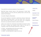
𝗖𝗼𝗻𝗻𝗲𝗰𝘁𝗶𝗻𝗴 𝗜𝗻𝗱𝘂𝘀𝘁𝗿𝗶𝗮𝗹 𝗽𝗿𝗼𝗱𝘂𝗰𝘁𝗶𝗼𝗻 𝘂𝗻𝗶𝘁𝘀 𝘁𝗼 𝘁𝗵𝗲 𝗳𝘂𝘁𝘂𝗿𝗲 Artificial intelligence (AI) is often discussed in abstract or futuristic terms, nonetheless at Stemix.Tech we believe in Applied AI Solutions - meaning intelligent solutions that improve real-world operations, now. We don't just use AI — we...

www.linkedin.com
View attachment 88990
Applied AI Solutions for industrial data collection and analysis
www.stemix.tech
View attachment 88988
View attachment 88981
View attachment 88982


 )
)
 ):
): 

